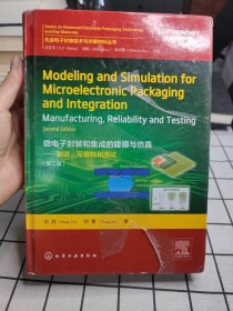


先进电子封装技术与关键材料丛书--微电子封装和集成的建模与仿真(英文版)
¥ 226 4.5折 ¥ 498 九品
仅1件
作者刘勇 著;刘胜
出版社化学工业出版社
出版时间2021-12
版次2
装帧精装
货号361
上书时间2024-05-19

- 店主推荐
- 最新上架


商品详情
- 品相描述:九品
图书标准信息
- 作者 刘勇 著;刘胜
- 出版社 化学工业出版社
- 出版时间 2021-12
- 版次 2
- ISBN 9787122392275
- 定价 498.00元
- 装帧 精装
- 开本 16开
- 纸张 胶版纸
- 页数 696页
- 字数 1.442千字
- 【内容简介】
-
随着电子封装的发展,电子封装已从传统的四个主要功能(电源系统、信号分布及传递、散热与机械保护)扩展为六个功能,即增加了DFX 及系统测试两个新的功能。其中DFX 是为“X”而设计,X 包括:可制造性、可靠性、可维护性、成本,甚至六西格玛。DFX 有望在产品设计阶段实现工艺窗口的确定、可靠性评估和测试结构及参数的设计等功能,真正做到“次就能成功”,从而将计算机辅助工程(CAE)变为计算机主导工程(CE),以大大加速产品的上市速度。本书是全面介绍DFX 在封装中应用的图书。作为封装工艺过程和快速可靠性评估及测试建模仿真的本专著,书中包含两位作者在工业界二十多年的丰富经验,以及在MEMS、IC和LED 封装部分成功的实例,希望能给国内同行起到抛砖引玉的作用。同时,读者将会从书中的先进工程设计和微电子产品的并行工程和协同设计方法中受益。
本书第2 版新增了两位作者在电子制造和封装领域新的成果与经验,例如电力电子模块的建模和仿真、电子封装耐热性的分析模型、3D TSV 封装等内容。
本书主要读者对象为学习DFX(制造工艺设计、测试设计、可靠性设计等)的研究人员、工程师和学生等。 - 【作者简介】
- 刘胜,武汉大学工业科学研究院,长江学者、科技部863计划、十一五重大项目“半导体照明工程”总体专家组成员,院长、教授,长江学者,博士生导师。1992年毕业于Stanford大学、获得博士学位。1998年在美国韦恩州立大学任终身副教授。2006年回国任华中科技大学教授,同时受聘于武汉光电国家实验室。目前是中国科技部“863计划”“十一五”半导体照明重大专项的11个专家之一, “863计划”“十五”微机电系统(MEMS)重大专项总体专家组成员5个专家之一。1995年获得美国白宫总统教授奖,1996年获得ASME青年工程师奖,1999年被评为中国海外杰出青年科学家。
- 【目录】
-
Foreword by Jianbin Luo xv
Foreword by C. P. xvii
Foreword by Zhigang Suo xix
Preface to Second Edition xxi
Preface to First Edition xxiii
Acknowledgments xxv
About the Authors xxvii
Part I Mechanics and Modeling 1
1 Constitutive Models and Finite Element Method 3
1.1 Constitutive Models for Typical Materials 3
1.1.1 Linear Elasticity 3
1.1.2 Elastic-Visco-Plasticity 5
1.2 Finite Element Method 9
1.2.1 Basic Finite Element Equations 9
1.2.2 Nonlinear Solution Methods 12
1.2.3 Advanced Modeling Techniques in Finite Element Analysis 14
1.2.4 Finite Element Applications in Semiconductor Packaging Modeling 17
1.3 Chapter Summary 18
References 19
2 Material and Structural Testing for Small Samples 21
2.1 Material Testing for Solder Joints 21
2.1.1 Specimens 21
2.1.2 A Thermo-Mechanical Fatigue Tester 23
2.1.3 Tensile Test 24
2.1.4 Creep Test 26
2.1.5 Fatigue Test 31
2.2 Scale Effect of Packaging Materials 32
2.2.1 Specimens 33
2.2.2 Experimental Results and Discussions 34
2.2.3 Thin Film Scale Dependence for Polymer Thin Films 39
2.3 Two-Ball Joint Specimen Fatigue Testing 41
2.4 Chapter Summary 41
References 43
3 Constitutive and User-Supplied Subroutines for Solders Considering Damage Evolution 45
3.1 Constitutive Model for Tin-Lead Solder Joint 45
3.1.1 Model Formulation 45
3.1.2 Determination of Material Constants 47
3.1.3 Model Prediction 49
3.2 Visco-Elastic-Plastic Properties and Constitutive Modeling of Underfills 50
3.2.1 Constitutive Modeling of Underfills 50
3.2.2 Identification of Material Constants 55
3.2.3 Model Verification and Prediction 55
3.3 A Damage Coupling Framework of Unified Viscoplasticity for the Fatigue of Solder Alloys 56
3.3.1 Damage Coupling Thermodynamic Framework 56
3.3.2 Large Deformation Formulation 62
3.3.3 Identification of the Material Parameters 63
3.3.4 Creep Damage 66
3.4 User-Supplied Subroutines for Solders Considering Damage Evolution 67
3.4.1 Return-Mapping Algorithm and FEA Implementation 67
3.4.2 Advanced Features of the Implementation 69
3.4.3 Applications of the Methodology 71
3.5 Chapter Summary 76
References 76
4 Accelerated Fatigue Life Assessment Approaches for Solders in Packages 79
4.1 Life Prediction Methodology 79
4.1.1 Strain-Based Approach 80
4.1.2 Energy-Based Approach 82
4.1.3 Fracture Mechanics-Based Approach 82
4.2 Accelerated Testing Methodology 82
4.2.1 Failure Modes via Accelerated Testing Bounds 83
4.2.2 Isothermal Fatigue via Thermal Fatigue 83
4.3 Constitutive Modeling Methodology 83
4.3.1 Separated Modeling via Unified Modeling 83
4.3.2 Viscoplasticity with Damage Evolution 84
4.4 Solder Joint Reliability via FEA 84
4.4.1 Life Prediction of Ford Joint Specimen 84
4.4.2 Accelerated Testing: Insights from Life Prediction 87
4.4.3 Fatigue Life Prediction of a PQFP Package 91
4.5 Life Prediction of Flip-Chip Packages 93
4.5.1 Fatigue Life Prediction with and without Underfill 93
4.5.2 Life Prediction of Flip-Chips without Underfill via Unified and Separated Constitutive Modeling 95
4.5.3 Life Prediction of Flip-Chips under Accelerated Testing 96
4.6 Chapter Summary 99
References 99
5 Multi-Physics and Multi-Scale Modeling 103
5.1 Multi-Physics Modeling 103
5.1.1 Direct-Coupled Analysis 103
5.1.2 Sequential Coupling 104
5.2 Multi-Scale Modeling 106
5.3 Chapter Summary 107
References 108
6 Modeling Validation Tools 109
6.1 Structural Mechanics Analysis 109
6.2 Requirements of Experimental Methods for Structural Mechanics Analysis 111
6.3 Whole Field Optical Techniques 112
6.4 Thermal Strains Measurements Using Moire Interferometry 113
6.4.1 Thermal Strains in a Plastic Ball Grid Array (PBGA) Interconnection 113
6.4.2 Real-Time Thermal Deformation Measurements Using Moire Interferometry 116
6.5 In-Situ Measurements on. Micro-Machined Sensors 116
6.5.1 Micro-Machined Membrane Structure in a Chemical Sensor 116
6.5.2 In-Situ Measurement Using Twyman-Green Interferometry 118
6.5.3 Membrane Deformations due to Power Cycles 118
6.6 Real-Time Measurements Using Speckle Interferometry 119
6.7 Image Processing and Computer Aided Optical Techniques 120
6.7.1 Image ftocessing for Fringe Analysis 120
6.7.2 Phase Shifting Technique for Increasing Displacement Resolution 120
6.8 Real-Time Thermal-Mechanical Loading Tools 123
6.8.1 Micro-Mechanical Testing 123
6.8.2 Environmental Chamber 124
6.9 Warpage Measurement Using PM-SM System 124
6.9.1 Shadow Moire and Project Moire Setup 125
6.9.2 Warpage Measurement of a BGA, TXvo Crowded PCBs 127
6.10 Chapter Summary 131
References 131
7 Application of Fracture Mechanics 135
7.1 Fundamental of Fracture Mechanics 135
7.1.1 Energy Release Rate 136
7.1.2 J Integral 138
7.1.3 Interfacial Crack 139
7.2 Bulk Material Cracks in Electronic Packages 141
7.2.1 Background 141
7.2.2 Crack Propagation in Ceramic/Adhesive/Glass System 142
7.2.3 Results 146
7.3 Interfacial Fracture Toughness 148
7.3.1 Background 148
7.3.2 Interfacial Fracture Toughness of Flip-Chip Package 0between Passivated Silicon Chip and Underfill 150
7.4 Three-Dimensional Energy Release Rate Calculation 159
7.4.1 Fracture Analysis 160
7.4.2 Results and Comparison 160
7.5 Chapter Summary 165
References 165
8 Concurrent Engineering for Microelectronics 169
8.1 Design Optimization 169
8.2 New Developments and Trends in Integrated Design Tools 179
8.3 Chapter Summary 183
References 183
Part II Modeling in Microelectronic Packaging and Assembly 185
9 Typical IC Packaging and Assembly Processes 187
9.1 Wafer Process and Thinning 188
9.1.1 Wafer Process Stress Models 188
9.1.2 Thin Film Deposition 189
9.1.3 Backside Grind for Thinning 191
9.2 Die Pick Up 193
9.3 Die Attach 198
9.3.1 Material Constitutive Relations 200
9.3.2 Modeling and Numerical Strategies 201
9.3.3 FEA Simulation Result of Flip-Chip Attach 204
9.4 Wire Bonding 206
9.4.1 Assumption, Material Properties and Method of Analysis 207
9.4.2 Wire Bonding Process with Different Parameters 208
9.4.3 Impact of Ultrasonic Amplitude 210
9.4.4 Impact of Ultrasonic Frequency 212
9.4.5 Impact of Friction Coefficients between Bond Pad and FAB 214
9.4.6 Impact of Different Bond Pad Thickness 217
9.4.7 Impact of Different Bond Pad Structures 217
9.4.8 Modeling Results and Discussion for Cooling Substrate Temperature after Wire Bonding 221
9.5 Molding 223
9.5.1 Molding Flow Simulation 223
9.5.2 Curing Stress Model 230
9.5.3 Molding Ejection and Clamping Simulation 236
9.6 Leadframe Forming/Singulation 241
9.6.1 Euler Forward versus Backward Solution Method 242
9.6.2 Punch Process Setup 242
9.6.3 Punch Simulation by ANSYS Implicit 244
9.6.4 Punch Simulation by LS-DYNA 246
9.6.5 Experimental Data 248
9.7 Chapter Summary 252
References 252
10 Opto Packaging and Assembly 255
10.1 Silicon Substrate Based Opto Package Assembly 255
10.1.1 State of the Technology 255
10.1.2 Monte Carlo Simulation of Bonding/Soldering Process 256
10.1.3 Effect of Matching Fluid 256
10.1.4 Effect of the Encapsulation 258
10.2 Welding of a Pump Laser Module 258
10.2.1 Module Description 258
10.2.2 Module Packaging Process Flow 258
10.2.3 Radiation Heat Transfer Modeling for Hermetic Sealing Process 259
10.2.4 Two-Dimensional FEA Modeling for Hermetic Sealing 260
10.2.5 Cavity Radiation Analyses Results and Discussions 262
10.3 Chapter Summary 264
References 264
11 MEMS and MEMS Package Assembly 267
11.1 A Pressure Sensor Packaging (Deformation and Stress) 267
11.1.1 Piezoresistance in Silicon 268
11.1.2 Finite Element Modeling and Geometry 270
11.1.3 Material Properties 270
11.1.4 Results and Discussion 271
11.2 Mounting of Pressure Sensor 273
11.2.1 Mounting Process 273
11.2.2 ModeUng 274
11.2.3 Results 276
11.2.4 Experiments and Discussions 277
11.3 Thermo-Fluid Based Accelerometer Packaging 279
11.3.1 Device Structure and Operation Principle 279
11.3.2 Linearity Analysis 280
11.3.3 Design Consideration 284
11.3.4 Fabrication 285
11.3.5 Experiment 285
11.4 Plastic Packaging for a Capacitance Based Accelerometer 288
11.4.1 Micro-Machined Accelerometer 289
11.4.2 Wafer-Level Packaging 290
11.4.3 Packaging of Capped Accelerometer 296
11.5 Tire Pressure Monitoring System (TPMS) Antenna 303
11.5.1 Test of TPMS System with Wheel Antenna 304
11.5.2 3D Electromagnetic Modeling of Wheel Antenna 306
11.5.3 Stress Modeling of Installed TPMS 307
11.6 Thermo-Fluid Based Gyroscope Packaging 310
11.6.1 Operating Principle and Design 312
11.6.2 Analysis of Angular Acceleration Coupling 313
11.6.3 Numerical Simulation and Analysis 314
11.7 Microjets for Radar and LED Cooling 316
11.7.1 Microjet Array Cooling System 319
11.7.2 Preliminary Experiments 320
11.7.3 Simulation and Model Verification 322
11.7.4 Comparison and Optimization of Three Micrqjet Devices 324
11.8 Air Flow Sensor 327
11.8.1 Operation Principle 329
11.8.2 Simulation of Flow Conditions 331
11.8.3 Simulation of Temperature Field on the Sensor Chip Surface 333
11.9 Direct Numerical Simulation of Particle Separation by Direct Current Dielectrophoresis 335
11.9.1 Mathematical Model and Implementation 335
11.9.2 Results and Discussion 339
11.10 Modeling of Micro-Machine for Use in Gastrointestinal Endoscopy 342
11.10.1 Methods 343
11.10.2 Results and Discussion 348
11.11 Chapter Summary 353
References 354
12 System in Package (SIP) Assembly 361
12.1 Assembly Process of Side by Side Placed SIP 361
12.1.1 Multiple Die Attach Process 361
12.1.2 Cooling Stress and Warpage Simulation after Molding 365
12.1.3 Stress Simulation in Trim Process 366
12.2 Impact of the Nonlinear Materials Behaviors on the Flip-Chip Packaging Assembly Reliability 370
12.2.1 Finite Element Modeling and Effect of Material Models 371
12.2.2 Experiment 374
12.2.3 Results and Discussions 375
12.3 Stacked Die Flip-Chip Assembly Layout and the Matenal Selection 381
12.3.1 Finite Element Model for the Stack Die FSBGA 383
12.3.2 Assembly Layout Investigation 385
12.3.3 Material Selection 389
12.4 Chapter Summary References Part m Modeling in Microelectronic Package and Integration: Reliability and Test 393
References 393
Part III Modeling in Microelectronic Package and Integration: Reliability and Test 395
13 Wafer Probing Test 397
13.1 Probe Test Model 397
13.2 Parameter Probe Test Modeling Results and Discussions 400
13.2.1 Impact of Probe Tip Geometry Shapes 401
13.2.2 Impact of Contact Friction 403
13.2.3 Impact of Probe Tip Scrub 403
13.3 Comparison Modeling: Probe Test versus Wire Bonding 406
13.4 Design of Experiment (DOE) Study and Correlation of Probing Experiment and FEA Modeling 409
13.5 Chapter Summary 411
References 412
14 Power and Thermal Cycling, Solder Joint Fatigue Life 413
14.1 Die Attach Process and Material Relations 413
14.2 Power Cycling Modeling and Discussion 413
14.3 Thermal Cycling Modeling and Discussion 420
14.4 Methodology of Solder Joint Fatigue Life Prediction 426
14.5 Fatigue Life Prediction of a Stack Die Flip-Chip on Silicon (FSBGA) 427
14.6 Effect of Cleaned and Non-Cleaned Situations on the Reliability of Flip-Chip Packages 434
14.6.1 Finite Element Models for the Clean and Non-Clean Cases 435
14.6.2 Model Evaluation 435
14.6.3 Reliability Study for the Solder Joints 437
14.7 Chapter Summary 438
References 439
15 Passivation Crack Avoidance 441
15.1 Ratcheting-Induced Stable Cracking: A Synopsis 441
15.2 Ratcheting in Metal Films 445
15.3 Cracking in Passivation Films 447
15.4 Design Modifications 449
15.5 Chapter Summary 452
References 452
16 Drop Test 453
16.1 Controlled Pulse Drop Test 453
16.1.1 Simulation Methods 454
16.1.2 Simulation Results 457
16.1.3 Parametric Study 458
16.2 Free Drop 460
16.2.1 Simulated Drop Test Procedure 460
16.2.2 Modeling Results and Discussion 461
16.3 Portable Electronic Devices Drop Test and Simulation 467
16.3.1 Test Set-Up 467
16.3.2 Modeling and Simulation 468
16.3.3 Results 470
16.4 Embedded Ultrathin Sensor Chip Drop Test and Simulation 471
16.4.1 Stress Sensor and Embedded Package 471
16.4.2 Drop Impact FEM Modeling and Validation 473
16.4.3 Parametric Study 476
16.5 Chapter Summary 482
References 483
17 Electromigration 485
17.1 Basic Migration Formulation and Algorithm 485
17.2 Electromigration Examples from IC Device and Package 489
17.2.1 A Sweat Structure 489
17.2.2 A Flip-Chip CSP with Solder Bumps 492
17.3 Chapter Summary 508
References 509
18 Popcorning in Plastic Packages 511
18.1 Statement of Problem 511
18.2 Analysis 513
18.3 Results and Comparisons 515
18.3.1 Behavior of a Delaminated Package due to Pulsed Heating-Verification 515
18.3.2 Convergence of the Total Strain Energy Release Rate 516
18.3.3 Effect of Delamination Size and Various Processes for a Thick Package 517
18.3.4 Effect of Moisture Expansion Coefficient 526
18.4 Chapter Summary 527
References 528
19 Modeling and Simulation of Power Electronic Modules 531
19.1 Structure Analysis of Power Electronics with Microchannel Coolers 531
19.2 Thermal Simulation of IGBT Module on Copper Microchannel Baseplate 533
19.3 Residual Stress Analysis of IGBT Module on Copper Microchannel Baseplate 538
19.4 Optimization for Warpage and Residual Stress Due to Reflow Process in IGBT Modules 547
19.4.1 Effects of Copper Layer Patterns of DBC on Warpage and Stress 548
19.4.2 Effects of the Arrangement of DBC Plates on Warpage and Residual Stress in IGBT Modules 549
19.4.3 Effects of the Thickness of Packaging Components on Warpage and Residual Stress in IGBT Modules 550
19.4.4 Effects of Pre-warped Copper Substrate on Warpage and Stress in IGBT Modules 551
19.4.5 Experiment 552
19.5 An Optimal Structural Design to Improve the Reliability of Al2O3-DBC Substrates under Thermal Cycling 554
19.5.1 Failure Mechanisms of DBC Substrate 556
19.5.2 Optimal Structure Design of DBC Substrate 558
19.5.3 Results and Discussion 562
19.6 Chapter Summary 565
References 565
20 Analytical Models for Thermal Resistances in Electronics Packaging 569
20.1 Resistances Eccentric Heat Source on Rectangular Plate with Convective Cooling at Upper and Lower Surfaces 569
20.1.1 Network Model 571
20.1.2 Comparisons and Discussion 575
20.2 Thermal Resistance Model for Calculating Mean Die Temperature of A Typical BGA Packaging 577
20.2.1 Model Development 578
20.2.2 Analysis and Calculation 587
20.2.3 Results and Discussions 589
20.3 Chapter Summary 590
References 590
21 3D Through Silicon Via (TSV) Packaging 593
21.1 A New Prewetting Process of TSV Electroplating for 3D Integration 593
21.1.1 Modeling and Simulation 593
21.1.2 Experiments 596
21.1.3 Results and Discussions 598
21.2 Study of Annular Copper-Filled TSVs of Sensor and Interposer Chips for
3D Integration 599
21.2.1 Experiments 600
21.2.2 Results and Discussion 602
21.3 Chapter Summary 608
References 608
Part IV Modern Modeling and Simulation Methodologies: Application to Nano Packaging 611
22 Classical Molecular Dynamics 613
22.1 General Description of Molecular Dynamics Method 613
22.2 Mechanism of Carbon Nanotube Welding onto the Metal 614
22.2.1 Computational Methodology 614
22.2.2 Results and Discussion 615
22.3 Applications of Car-Parrinello Molecular Dynamics 622
22.3.1 Car-Parrinello Simulation of Initial Growth Stage of Gallium Nitride
on Carbon Nanotube 622
22.3.2 Effects of Mechanical Deformation on Outer Surface Reactivity of Carbon Nanotubes 626
22.3.3 Adsorption Configuration of Magnesium on Wurtzite Gallium Nitride Surface Using First-Principles Calculations 631
22.4 Nano-Welding by RF Heating 636
22.5 Chapter Summary 640
References 640
23 Aluminum Nitride Deposition 645
23.1 Study Effects of Temperature and N: Al Flux Ratio on Deposited AlN 645
23.1.1 Model and Methods 645
23.1.2 Results and Discussion 647
23.2 AlN Deposition on GaN Substrate 653
Contents xiii
23.2.1 Analysis Methods 654
23.2.2 Results and Discussion 655
23.3 Atomic Simulation of AlGaN Film Deposition on AlN Template 662
23.3.1 Analysis Methods 662
23.3.2 Results and Discussion 662
23.4 Chapter Summary 667
References 667
24 Mechanical Properties of AlN and Graphene 671
24.1 Mechanical Properties of AlN with Raman Verification 671
24.1.1 Methodology 672
24.1.2 Results and Analysis 672
24.2 Stress Evolution in AlN and GaN Grown on Si(111): Experiments and Theoretical Modeling 676
24.2.1 Sample Preparation and Material Characteristics 677
24.2.2 Stress Characterization 679
24.2.3 Simulations 681
24.3 Molecular Distinctive Nanofriction of Graphene Coated Copper Foil 685
24.3.1 Modeling and Method 686
24.3.2 Results and Discussion 687
24.4 Chapter Summary 691
References 692
Appendix Conversion Tables and Constants 696

相关推荐
-
电子封装技术与应用/PCB先进制造技术
全新南京
¥ 109.02
-

先进电子封装技术与关键材料丛书--FreeformOpticsforLEDPackage
全新广州
¥ 236.36
-
先进电子封装技术与关键材料丛书--FreeformOpticsforLEDPackage
全新济宁
¥ 151.48
-
先进电子封装技术与关键材料丛书--FreeformOpticsforLEDPackage
全新保定
¥ 143.00
-
先进电子封装技术与关键材料丛书--FreeformOpticsforLEDPackage
全新潍坊
¥ 155.00
-

先进电子封装技术与关键材料丛书--FreeformOpticsforLEDPackage
全新无锡
¥ 200.49
-

先进电子封装技术与关键材料丛书--FreeformOpticsforLEDPackage
全新廊坊
¥ 98.00
-
先进电子封装技术与关键材料丛书--FreeformOpticsforLEDPackage
全新廊坊
¥ 100.00
-

先进电子封装技术与关键材料丛书--FreeformOpticsforLEDPackage
九品杭州
¥ 76.00
-

先进电子封装技术与关键材料丛书--FreeformOpticsforLEDPackage
八五品北京
¥ 70.00
— 没有更多了 —
以下为对购买帮助不大的评价