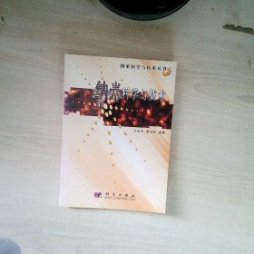
纳米科学与技术
实物拍照,所见即所得,放心直接拍,能拍就有货
¥ 24.11 3.7折 ¥ 65 九品
仅1件
河北保定
认证卖家担保交易快速发货售后保障
作者[英]凯索尔(Kelsall)
出版社科学出版社
出版时间2007-01
版次1
装帧平装
货号9787030182579
上书时间2024-12-13
- 在售商品 暂无
- 平均发货时间 9小时
- 好评率 暂无
- 店主推荐
- 最新上架
商品详情
- 品相描述:九品
图书标准信息
- 作者 [英]凯索尔(Kelsall)
- 出版社 科学出版社
- 出版时间 2007-01
- 版次 1
- ISBN 9787030182579
- 定价 65.00元
- 装帧 平装
- 开本 其他
- 纸张 胶版纸
- 页数 456页
- 字数 747千字
- 【内容简介】
-
本书覆盖了从电磁微纳结构到分子自组织以及生物微纳技术的整个微纳技术领域,由该领域内的专家组撰写,包括了微纳米科学技术的各个方面,互相紧密联系,并可前后对照。
本书保持了多学科性,涉及到物理、化学、生物学、材料科学、电子工程等多个学科,有以下特点:循序渐进的介绍了微纳米科学,覆盖面广,具有教科书的风格;采用举例的方式介绍了微纳米科学各个领域的研究结果,所用的例子都是非常有代表性的研究结果;讨论了微纳米科学技术今后发展的特点和主要突破口。
本书为刚刚进入微纳米技术领域的读者提供了非常有价值的资料,适合于微纳米技术相关专业的研究生、博士生参考,并可作为该专业博士后的参考书,还可以供毕业课题与微纳米技术相关的毕业生做参考。 - 【目录】
-
1 Generic methodologies for nanotechnology: classification and fabrication
1.1 Introduction and classification
1.1.1 What is nanotechnology?
1.1.2 Classification of nanostructures
1.1.3 Nanoscale architecture
1.2 Summary of the electronic properties of atoms and solids
1.2.1 The isolated atom
1.2.2 Bonding between atoms
1.2.3 Giant molecular solids
1.2.4 The free electron model and energy bands
1.2.5 Crystalline solids
1.2.6 Periodicity of crystal lattices
1.2.7 Electronic conduction
1.3 Effects of the nanometre length scale
1.3.1 Changes to the system total energy
1.3.2 Changes to the system structure
1.3.3 How nanoscale dimensions affect properties
1.4 Fabrication methods
1.4.1 Top-down processes
1.4.2 Bottom-up processes
1.4.3 Methods for templating the growth of nanomaterials
1.4.4 Ordering of nanosystems
1.5 Preparation, safety and storage issues
Bibliography
2 Generic methodologies for nanotechnology: characterization
2.1 General classification of characterization methods
2.1.1 Analytical and imaging techniques
2.1.2 Some scattering physics
2.2 Microscopy techniques
2.2.1 General considerations for imaging
2.2.2 Image magnification and resolution
2.2.3 Other considerations for imaging
2.2.4 Light microscopy
2.3 Electron microscopy
2.3.1 General aspects of electron optics
2.3.2 Electron beam generation
2.3.3 Electron-specimen interactions
2.3.4 Scanning electron microscopy
2.3.5 Transmission electron microscopy
2.3.6 Scanning transmission electron microscopy
2.4 Field ion microscopy
2.5 Scanning probe techniques
2.5.1 Scanning tunnelling microscopy
2.5.2 Atomic force microscopy
2.5.3 Other scanning probe techniques
2.6 Diffraction techniques
2.6.1 Bulk diffraction techniques
2.6.2 Surface diffraction techniques
2.7 Spectroscopy techniques
2.7.1 Photon spectroscopy
2.7.2 Radio frequency spectroscopy
2.7.3 Electron spectroscopy
2.8 Surface analysis and depth profiling
2.8.1 Electron spectroscopy of surfaces
2.8.2 Mass spectrometry of surfaces
2.8.3 Ion beam analysis
2.8.4 Reflectometry
2.9 Summary of techniques for property measurement
2.9.1 Mechanical properties
2.9.2 Electron transport properties
2.9.3 Magnetic properties
2.9.4 Thermal properties
Bibliography
3 Inorganic semiconductor nanostructnres
3.1 Introduction
3.2 Overview of relevant semiconductor physics
3.2.1 What is a semiconductor?
3.2.2 Doping
3.2.3 The concept of effective mass
3.2.4 Carrier transport, mobility and electrical conductivity
3.2.5 Optical properties of semiconductors
3.2.6 Excitons
3.2.7 The pn junction
3.2.8 Phonons
3.2.9 Types of semiconductor
3.3 Quantum confinement in semiconductor nanostructures
3.3.1 Quantum confinement in one dimension: quantum wells
3.3.2 Quantum confinement in two dimensions: quantum wires
3.3.3 Quantum confinement in three dimensions: quantum dots
3.3.4 Superlattices
3.3.5 Band offsets
3.4 The electronic density of states
3.5 Fabrication techniques
3.5.1 Requirements for an ideal semiconductor nanostructure
3.5.2 The epitaxial growth of quantum wells
3.5.3 Lithography and etching
3.5.4 Cleaved-edge overgrowth
3.5.5 Growth on vicinal substrates
3.5.6 Strain-induced dots and wires
3.5.7 Electrostatically induced dots and wires
3.5.8 Quantum well width fluctuations
3.5.9 Thermally annealed quantum wells
3.5.10 Semiconductor nanocrystals
3.5.11 Colloidal quantum dots
3.5.12 Self-assembly techniques
3.5.13 Summary of fabrication techniques
3.6 Physical processes in semiconductor nanostructures
3.6.1 Modulation doping
3.6.2 The quantum Hall effect
3.6.3 Resonant tunnelling
3.6.4 Charging effects
3.6.5 Ballistic carrier transport
3.6.6 Interband absorption in semiconductor nanostructures
3.6.7 Intraband absorption in semiconductor nanostructures
3.6.8 Light emission processes in nanostructures
3.6.9 The phonon bottleneck in quantum dots
3.6.10 The quantum confined Stark effect
3.6.11 Non-linear effects
3.6.12 Coherence and dephasing processes
3.7 The characterisation of semiconductor nanostructures
3.7.1 Optical and electrical characterisation
3.7.2 Structural characterisation
3.8 Applications of semiconductor nanostructures
3.8.1 Injection lasers
3.8.2 Quantum cascade lasers
3.8.3 Single-photon sources
3.8.4 Biological tagging
3.8.5 Optical memories
3.8.6 Impact of nanotechnology on conventional electronics
3.8.7 Coulomb blockade devices
3.8.8 Photonic structures
3.9 Summary and outlook
Bibliography
4 Nanomagnetic materials and devices
4.1 Magnetism
4.1.1 Magnetostatics
4.1.2 Diamagnetism, paramagnetism and ferromagnetism
4.1.3 Magnetic anisotropy
4.1.4 Domains and domain wails
4.1.5 The magnetization process
4.2 Nanomagnetic materials
4.2.1 Particulate nanomagnets
4.2.2 Geometrical nanomagnets
4.3 Magnetoresistance
4.3.1 Contributions to resistivity in metals
4.3.2 Giant magnetoresistance
4.3.3 Spin valves
4.3.4 Tunnelling magnetoresistance
4.4 Probing nanomagnetic materials
4.5 Nanomagnetism in technology
4.6 The challenges facing nanomagnetism
Bibliography
5 Processing and properties of inorganic nanomaterials
5.1 Introduction
5.1.1 Classification
5.2 The thermodynamics and kinetics of phasetransformations
5.2.1 Thermodynamics
5.2.2 Homogeneous nucleation
5.2.3 Heterogeneous nucleation
5.2.4 Growth
5.2.5 Overall transformation rate
5.3 Synthesis methods
5.3.1 Rapid solidification processing from the liquid state
5.3.2 Devitrification
5.3.3 Inert gas condensation
5.3.4 Electrodeposition
5.3.5 Mechanical methods
5.4 Structure
5.4.1 Microstructure
5.4.2 Grain boundary structure
5.4.3 Structural metastability
5.5 Microstructural stability
5.5.1 Diffusion
5.5.2 Grain growth
5.5.3 Zener pinning
5.5.4 Solute drag
5.6 Powder consolidation
5.6.1 Compaction of nanopowders
5.6.2 Sintering
5.6.3 Role of impurities
5.6.4 Porosity
5.6.5 Non-conventional processing
5.7 Mechanical properties
5.7.1 Hardness and strength
5.7.2 Ductility and toughness
5.7.3 Creep and superplasticity
5.8 Ferromagnetic properties
5.8.1 Fundamental magnetic properties
5.8.2 Nanocomposite soft magnetic materials
5.8.3 Hard magnetic materials
5.9 Catalytic properties
5.10 Present and potential applications for nanomaterials
5.10.1 Ultraviolet absorbers
5.10.2 Magnetic applications
5.10.3 Coatings
Bibliography
6 Electronic and electro-optic molecular materials and devices
6.1 Concepts and materials
6.1.1 The solid state: crystals and glasses
6.1.2 Chemistry of carbon
6.1.3 Examples of organic semiconductors
6.1.4 Excitations in organic semiconductors
6.1.5 Charge carrier injection and transport
6.1.6 Polymers versus small molecules
6.1.7 Organic metals?
6.2 Applications and devices
6.2.1 Synthetic metals
6.2.2 Organic field effect transistors
6.2.3 Organic light-emitting devices
6.2.4 Organic photovoltaics
6.3 Carbon nanotubes
6.3.1 Structure
6.3.2 Synthesis
6.3.3 Electronic properties
6.3.4 Vibrational properties
6.3.5 Mechanical properties
6.3.6 Applications
Appendix: Reference table of organic semiconductors
Bibliography
7 Self-assembling nanostructured molecular materials and devices
7.1 Introduction
7.2 Building blocks
7.2.1 Synthetic
7.2.2 Biological
7.3 Principles of self-assembly
7.3.1 Non-covalent interactions
7.3.2 Intermolecular packing
7.3.3 Biological self-assembly
7.3.4~ Nanomotors
7.4 Self-assembly methods to prepare and pattern nanoparticles
7.4.1 Nanoparticles from micellar and vesicular polymerization
7.4.2 Functionalized nanoparticles
7.4.3 Colloidal nanoparticle crystals
7.4.4 Self-organizing inorganic nanoparticles
7.4.5 Liquid crystal nanodroplets
7.4.6 Bionanoparticles
7.4.7 Nano-objects
7.5 Templated nanostructures
7.5.1 Mesoporons silica
7.5.2 Biomineralization
7.5.3 Nanostructures templated by block copolymer self-assembly
7.6 Liquid crystal mesophases
7.6.1 Micelles and vesicles
7.6.2 LameUar phase
7.6.3 ABC triblock structures
7.6.4 Smectic and nematic liquid crystals
7.6.5 Discotic liquid crystals
7.7 Summary and outlook
Bibliography
8 Maeromolecules at interfaces and structured organic films
8.1 Macromolecules at interfaces
8.2 The principles of interface science
8.2.1 Surface and interface energies
8.3 The analysis of wet interfaces
8.4 Modifying interfaces
8.4.1 Adsorption and surfactancy
8.4.2 Polymer adsorption
8.4.3 The chemistry of grafting
8.4.4 Physical properties of grafted polymer layers
8.4.5 Nanostructured organic coatings by soft lithography and other techniques
8.5 Making thin organic films
8.5.1 Spin-coating of polymers and colloids
8.5.2 Making organic multilayers
8.6 Surface effects on phase separation
8.6.1 Polymer blends
8.6.2 Block copolymers
8.7 Nanopatterning surfaces by self-assembly
8.7.1 Patterns produced on heterogeneous substrates
8.7.2 Topographically patterned surfaces
8.7.3 Patterns produced by thin film dewetting
8.8 Practical nanoscale devices exploiting macromolecules at interfaces
8.8.1 Molecular and macromolecular electronics
8.8.2 Nanofhiidics
8.8.3 Filtration and sorting
Bibliography
9 Bionanotechnology
9.1 New tools for investigating biological systems
9.1.1 Scanning probe microscopy for biomolecular imaging
9.1.2 Force measurement in biological systems
9.1.3 Miniaturisation and analysis
9.1.4 0rganisation of biomolecular structure at the nanometre scale
9.2 Biomimetic nanotechnology
9.2.1 DNA as a nanotechnology building block
9.2.2 Molecular motors
9.2.3 Artificial photosynthesis
9.3 Conclusions
Bibliography
Index
点击展开
点击收起
相关推荐
— 没有更多了 —


以下为对购买帮助不大的评价