


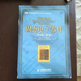
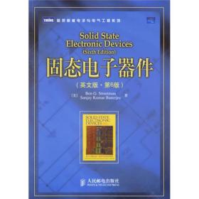
固态电子器件(英文版)(第6版)
有污垢
¥ 118 九品
仅1件
安徽阜阳
认证卖家担保交易快速发货售后保障
作者[美]斯特里特曼、[美]巴纳里杰 著
出版社人民邮电出版社
出版时间2007-02
版次1
装帧平装
货号2-68
上书时间2021-04-20


商品详情
- 品相描述:九品
图书标准信息
- 作者 [美]斯特里特曼、[美]巴纳里杰 著
- 出版社 人民邮电出版社
- 出版时间 2007-02
- 版次 1
- ISBN 9787115155481
- 定价 65.00元
- 装帧 平装
- 开本 16开
- 纸张 胶版纸
- 页数 581页
- 字数 720千字
- 丛书 图灵原版电子与电气工程系列
- 【内容简介】
-
本书是介绍半导体器件工作原理的经典入门教材,其主要内容包括固体物理基础和半导体器件物理两大部分,同时也涵盖半导体晶体结构与材料生长技术、集成电路原理与制造工艺以及光电子器件与高频大功率器件等相关内容。
本书注重基本物理概念,强调理论联系实际,可作为高等院校电子信息类专业“固态器件与电路”专业基础课的教材,也可供相关领域的研究人员和技术人员参考。 - 【作者简介】
- BenG.Streetman是美国国家工程院院士和美国艺术与科学院院士,IEEE会士和美国电化学学会(ECS)会士。现任美国得克萨斯大学奥斯汀分校工学院院长和该鹇电机工程与计算机工程讲座教授,也是该校微电子研究中心的创始人和第一任主任(1984年-1996年)。Streetman教授的教学领域和研究兴趣主要包括半导体材料与半导体器件两个方面。
- 【目录】
-
1CRYSTALPROPERTIESANDGROWTHOFSEMICONDUCTORS
1.1SemiconductorMaterials
1.2CrystalLattices
1.2.1PeriodicStructures
1.2.2CubicLattices
1.2.3PlanesandDirections
1.2.4TheDiamondLattice
1.3BulkCrystalGrowth
1.3.1StartingMaterials
1.3.2GrowthofSingle-CrystalIngots
1.3.3Wafers
1.3.4Doping
1.4EpitaxialGrowth
1.4.1Lattice-MatchinginEpitaxialGrowth
1.4.2Vapor-PhaseEpitaxy
1.4.3MolecularBeamEpitaxy
2ATOMSANDELECTRONS
2.1IntroductiontoPhysicalModels
2.2ExperimentalObservations
2.2.1ThePhotoelectricEffect
AtomiSpectra
2.3TheBohrModlel
2.4QuantumMechanics
2.4.1ProbabilityandtheUncertaintyPrinciple
2.4.2TheSchr6dingerWaveEquation
2.4.3PotentialWellProblem
2.4.4Tunneling
2.5AtomicStructureandthePeriodiclable
2.5.1TheHydrogenAtom
2.5.2ThePeriodicTable
3ENERGYBANDSANDCHARGECARRIERSINSEMICONDUCTORS
3.1BondingForcesandEnergyBandsinSolids
3.1.1BondingForcesinSolids
3.1.2EnergyBands
3.1.3Metals,Semiconductors,andInsulators
3.1.4DirectandIndirectSemiconductors
3.1.5Variationo!EnergyBandswithAIIoComposition
3.2ChargeCarriersSemiconductors
3.2.1ElectronsandHoles
3.2.2EffectiveMass
3.2.3IntrinsicMaterial
3.2.4ExtrinsicMaterial
3.2.5ElectronsandHolesinQuantumWells
3.3CarrierConcentrations
3.3.1TheFermiLevel
3.3.2ElectronandHoleConcentrationsatEquilibrium
3.3.3TemperatureDependenceofCarrierConcentrations
3.3.4CompensationandSpaceChargeNeutrality
3.4DriftofCarriersinElectricandMagneticFields
3.4.1ConductivityandMobility
3.4.2DriftandResistance
3.4.3EffectsoflemperatureandDopingonMobility
3.4.4High-FieldEffects
3.45TheHallEffect
3.5InvarianceoftheFermiLevelatEquilibrium
EXCESSCARRIERSINSEMICONDUCTORS
4.1OpticalAbsorption
4.2Luminescence
4.2.1Photoluminescence
4.2.2Electroluminescence
4.3CarrierLifetimeandPhotoconductivity
4.3.1DirectRecombinationofElectronsandHoles
4.3.2IndirectRecombination;Trapping
4.3.3SteadyStateCarrierGeneration;Quasi-FermiLevels
4.34PhotoconductiveDevices
4.4DiffusionofCarriers
4.4.1DiffusionProcesses
4.4.2DiffusionandDriftofCarriers;Built-inFields
4.4.3DiffusionandRecombination;TheContinuityEquation
4.4.4SteadyStateCarrierInjection;DiffusionLength
4.4.5TheHaynes-ShockleyExperiment
4.4.6GradientsintheQuasi-FermiLevels
5JUNCTIONS
5.1Fabricationofp-nJunctions
5.1.1ThermalOxidation
5.1.2Diffusion
5.1.3RapidThermalProcessing
5.1.4IonImplantation
5.1.5ChemicalVaporDeposition(CVD)
5.1.6Photolithography
5.1.7Etching
5.1.8Metallization
5.2EquilibriumConditions
5.2.1TheContactPotential
5.2.2EquilibriumFermiLevels
5.2.3SpaceChargeataJunction
5.3Forward-andReverse-BiasedJunctions;SteadyStateConditions
5.3.1QualitativeDescriptionofCurrentFlowataJunction
5.3.2CarrierInjection
5.3.3ReverseBias
5.4Reverse-BiasBreakdown
5.4.1ZenerBreakdown
5.4.2AvalancheBreakdown
5.4.3Rectifiers
5.4.4TheBreakdownDiode
5.5TransientandA-CConditions
5.5.1TimeVariationofStoredCharge
5.5.2ReverseRecoveryTransient
5.5.3SwitchingDiodes
5.5.4Capacitanceofp-njunctions
5.5.5TheVaractorDiode
5.6DeviationsfromtheSimplTheory
5.6.1EffectsofContactPotentialonCarrierInjection
5.6.2RecombinationandGenerationintheTransitionRegion
5.6.3OhmicLosses
5.6.4GradedJunctions
5.7Metal-SemiconductorJunctions
5.7.1SchottkyBarriers
5.7.2RectifyingContacts
5.7.3OhmicContacts
5.7.4lypicalSchottkyBarriers
5.8Heterojunctions
6FIELD-EFFECTTRANSISTORS
6.1TransistorOperation
6.1.1TheLoadLine
6.1.2Amplificationa4dSwitching
6.2TheJunctionFET
6.2.1Pinch-offandSaturation
6.2.2GateControl
6.2.3Current-VoltageCharacteristics
6.3TheMetaI-SemiconductorFET
6.3.1TheGaAsMESFET
6.3.2TheHighElectronMobilityTransistor(HEMT)
6.3.3ShortChannelEffects
6.4TheMetal-Insulator-SemiconductorFET
6.4.1BasicOperationandFabrication
6.4.2TheIdealMOSCapacitor
6.4.3EffectsofRealSurfaces
6.4.4ThresholdVoltage
6.4.5MOSCapacitance-VoltageAnalysis
6.4.6Time-DependentCapacitanceMeasurements
6.4.7Current-VoltageCharacteristicsofMOSGateOxides
6.5TheMOSField-EffectTrans~stor
6.5.1OutputCharacteristics
6.5.2TransferCharacteristics
6.5.3MobilityModels
6.5.4ShortChannelMOSFETI-VCharacteristics
6.5.5ControlofThresholdVoltage
6.5.6SubstrateBiasEffects
6.5.7SubthresholdCharacteristics
6.5.8EquivalentCircuitfortheMOSFET
6.5.9MOSFETScalingandHotElectronEffects
6.5.10Drain-inducedBarrierLowering
6.5.11ShortChannelEffectandNarrowWidthEffect
6.5.12Gate-InducedDrainLeakage
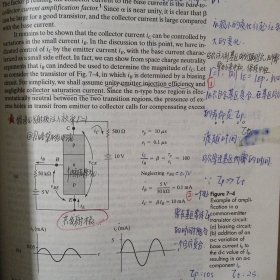
7BIPOLARJUNCTIONTRANSISTORS
7.1Fundamentalso!BJTOperation
7.2AmplificationwithBJTs
7.3BJTFabrication
7.4MinorityCarrierDistributionsandTerminalCurrents
7.4.1SolutionoftheDiffusionEquationintheBaseRegion
7.4.2EvaluationoftheTerminalCurrents
7.4.3ApproximationsoftheTerminalCurrents
7.4.4CurrentTransferRatio
7.5GeneralizedBiasing
7.5.1TheCoupled-DiodeModel
7.5.2ChargeControlAnalysis
7.6Switching
7.6.1Cutoff
7.6.2Saturation
7.6.3TheSwitchingCycle
7.6.4SpecificationsforSwitchingTransistors
7.7OtherImportantEffects
7.7.1DriftintheBaseRegion
7.7.2BaseNarrowing
7.7.3AvalancheBreakdown
7.7.4InjectionLevel;ThermalEffects
7.7.5BaseResistanceandEmitterCrowding
7.7.6GummeI-PoonModel
7.77KirkEffect
7.8FrequencyLimitationsofTransistors
7.8.1CapacitanceandChargingTimes
7.8.2TransitTimeEffects
7.8.3WebsterEffect
7.8.4High-FrequencyTransistors
7.9HeterojunctionpolarTransistors
8OPTOELECTRONICDEVICES
8.1Photodiodes
8.1.1CurrentandVoltageinanIlluminatedJunction
8.1.2SolarCells
8.1.3Photodetectors
8.1.4Gain,Bandwidth,andSignal-to-NoiseRatioofPhotodetectors
8.2Light-EmittingDiodes
8.2.1Light-EmittingMaterials
8.2.2Fiber-OpticCommunications
8.3Lasers
8.4SemiconductorLasers
8.4.1PopulationInversionataJunction
8.4.2EmissionSpectraforp-nJunctionLasers
8.4.3TheBasicSemiconductorLaser
8.4.4HeterojunctionLasers
8.4.5MaterialsforSemiconductorLasers
9INTEGRATEDCIRCUITS
9.1Background
9.1.1AdvantagesofIntegration
9.1.2TypesofIntegratedCircuits
9.2EvolutionoflntegratedCircuits
9.3MonolithicDeviceElements
9.3.1CMOSProcessIntegration
9.3.2Silicon-on-Insulator(SOl)
9.3.3IntegrationofO.therCircuitElements
9.4argeTransferDevices
9.4.1DynamicEffectsinMOSCapacitors
9.4.2TheBasicCCD
9.4.3ImprovementsontheBasicStructure
9.4.4App_licationsofCCDs
9.5UltraLargeScalelntegration(ULSI)
9.5.1LogicDevices
9.5.2SemiconductorMemories
9.6resting,Bonding,andPackaging
9.6.1Testing
9.6.2WireBonding
9.6.3Flip-ChipTechniques
9.6.4Packaging
1OHIGH-FREQuENCYANDHIGH-POWERDEVICES
10.1TunnelDiodes
10.1.1DegenerateSemiconductors
10.2TheIMPATTDiode
10.3TheGunnDiode
10.3.1TheTransferred-ElectronMechanism
10.3.2FormationandDriftofSpaceChargeDomains
10.4Thep-n-p-nDiode
10.4.1BasicStructure
10.4.2TheTwo-TransistorAnalogy
10.4.3VariationofαwithInjection
10.4.4Forward-BlockingState
10.4.5ConductingState524
10.4.6TriggeringMechanisms
10.5TheSemiconductor-Controllerectifier
10.5.1TurningofftheSCR
10.6Insulated-GateBipolarTransistor
APPENDICES
Ⅰ.DefinitionsofCommonlyUsedSymbols
Ⅱ.PhysicalConstantsandConversionFactors
Ⅲ.PropertiesofSemiconductorMaterials
Ⅳ.DerivationoftheDensityofStatesintheConductionBand
Ⅴ.DerivationofFermi-DiracStatistics
Ⅵ.DryandWetThermalOxideThicknessGrownon
Si(100)asaFunctionofTimeand.lemperature
Ⅶ.SolidSolubilitiesofImpuritiesin
Ⅶ.DiffusivitiesofDopantsinSiandSiO2
Ⅸ.ProjectedRangeandStraggleasFunctionof
ImplantEnergyinSi
ANSWERSTOSELECTEDSELFQUIZQUESTIONS
INDEX
点击展开
点击收起

相关推荐


— 没有更多了 —
以下为对购买帮助不大的评价